Dielectric Etchers Market Size
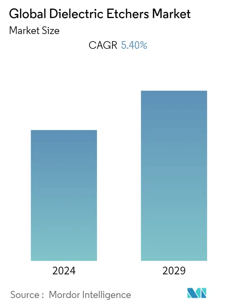
| Study Period | 2019 - 2029 |
| Base Year For Estimation | 2023 |
| CAGR | 5.40 % |
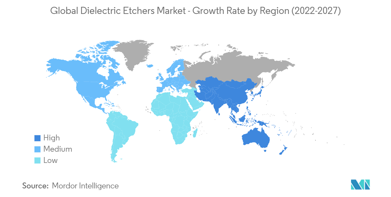
| Fastest Growing Market | Asia Pacific |
| Largest Market | Asia Pacific |
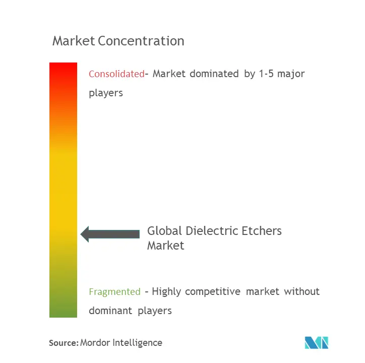
| Market Concentration | Low |
Major Players
*Disclaimer: Major Players sorted in no particular order |
Dielectric Etchers Market Analysis
The Global Dielectric Etchers Market is expected to register a CAGR of 5.4% during the forecast period 2022 to 2027. The increasing demand for miniaturizing the ICs to be used in compact & mobile devices is expected to drive the market. The current electronic devices use semiconductors of circuit line width, which ranges from 5 - 20 nm; however, the emergence of atomic-level etching process & demand for miniaturized IC, which consumes less power, will push the circuit line width range to 0 - 10 nm.
- An increase in demand for neuromorphic chips will drive the market for etchers. The rising demand for artificial intelligence, data processing & analytics is a major factor influencing the innovation & adoption of neuromorphic chips across the globe. Etch techniques aid in creating chip features by eliminating coatings and materials put on the wafer selectively. These procedures entail producing increasingly small and intricate features with difficult-to-remove material combinations.
- The latest trend in the global dielectric etchers market is the emergence of 3D ICs. With the increasing demand for faster computing devices that consume less amount of energy will significantly drive the demand for 3D chip stacking. The growing need for miniaturizing electronic devices in fields such as Aerospace, Automotive & Medical sectors will drive the demand for dielectric etchers, which are capable of altering structures to a precision of 0 - 10 nm & even at an atomic level.
- Etch methods also produce tall, high-aspect-ratio features, like through-silicon vias (TSVs), which allow chip packaging and micro-electromechanical system integration (MEMS). For instance, Lam Research plasma etch systems provide high-performance and high-productivity capabilities required to build precise structures, ranging from tall and narrow, short and wide, to a few angstroms in size.
- In May 2021, Applied Materials, Inc. announced three new materials engineering solutions that enable its memory customers three new options to scale DRAM and optimize chip performance, power, area, cost, and time to market (PPACt). DRAM manufacturers use black diamond, a low-k dielectric material developed by Applied Materials, to solve logic interconnect scalability problems.
- The outbreak of COVID-19 significantly disrupted the supply chain and production during the initial phase of 2020. The impact was more severe for semiconductor manufacturers, the major end users for semiconductor etch equipment. Due to labor shortages, many players in the semiconductor supply chain had to reduce or even suspend their operations. The industry was riddled with a high deficit and increasing demand, which led to a significant supply chain gap. The initial spread of the virus led to the shutting down or reduction of foundry capacity utilization, fearing the decreasing demand for chips across major sectors, like the automotive. Diminished output led to a global shortage of semiconductors as demand increased, despite the initial estimates by semiconductor foundries.
Dielectric Etchers Market Trends
This section covers the major market trends shaping the Dielectric Etchers Market according to our research experts:
Demand for Neuromorphic Chip to Boost Dielectric Etchers Market
- A neuromorphic chip is a data processor inspired by biological brain processing ability to achieve high-speed & low power learning and constructed with capabilities of millions of neurons. The size of these chips is small enough to go mobile, and applications are broad.
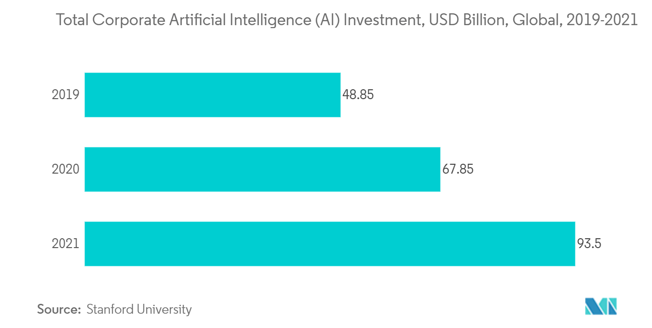
- Besides, AI-based startups are increasing day by day. The technologies enabled by AI require neuromorphic chips for processing. Therefore, the rising demand for artificial intelligence, data processing & analytics is a major factor influencing the innovation & adoption of neuromorphic chips across the globe, which in turn is expected to drive the market for dielectric etchers.
- The rising demand for artificial intelligence, data processing, and analytics is a significant factor that drives the adoption of neuromorphic chips worldwide, thereby creating the need for dielectric etchers. Moreover, rapid technological upgradation of Internet of Things applications for advanced intelligent devices is also anticipated to boost the demand for technologically advanced semiconductors. This, in turn, is predicted to create significant demand for dielectric etching in the market.
- DRAM is in high demand due to the global economy's digital transition. The Internet of Things creates significant additional computer devices at the edge, resulting in an exponential rise in data that is transported to the cloud for processing. The industry needs advancements that would allow DRAM to scale down in size and cost while running at greater speeds and consuming less power, which drives the market growth.
- Smartphones and other applications in the consumer electronics market that require semiconductor ICs drive the demand for dielectric etcher. Furthermore, as the number of Internet of Things (IoT) devices grows, the semiconductor industry aims to invest in this technology to produce more innovative products.
Asia Pacific Region to Hold a Significant Share
- Integrated Device Manufacturers (IDM) such as Qualcomm, Broadcom Ltd., Nvidia, MediaTek, Apple, AMD, etc. across the globe are adopting fabless business model, where the organization will design the chipset layout and outsource the manufacturing to chipset manufacturers such as TSMC, UMC & SMIC. The fabless business model helps organizations to concentrate their efforts on investing profits in research and development of new technologies while maintaining the high production volumes needed to maintain sales.
- Organizations such as TSMC, UMC, DB Hitek, SMIC, etc. utilize their foundries to produce the chipset according to the specifications and volumes requirement of the customers. A major share of these foundries operates from China, Taiwan & South Korea.
- Atomic layer etching (ALE) is a sophisticated etching process that provides superior depth control on shallow structures. As device feature size shrinks, ALE becomes increasingly necessary to attain the accuracy required for enhanced performance.
- The production of advanced microelectronic devices requires high-fidelity pattern transfer (etching). As features drop to sub-10nm sizes and new devices use ultra-thin 2D materials, atomic-scale accuracy becomes more important. This raised the demand for atomic layer etching (ALE), a technique that overcomes the limits of traditional (continuous) etching at the atomic level.
- TSMC has been Apple's exclusive manufacturer of Apple's A-series chips. This chipset will be fabricated using a 7-nanometer chipset called A13. Besides, with automotive electronics industry flourishing exceedingly in the region, Asia-Pacific is providing a plethora of opportunities for market growth.
Dielectric Etchers Industry Overview
The Gloabl Dielectric Etchers Market is very competitive in nature. The market is highly concentrated due to the presence of various small and large players. All the major players account for a large share of the market and are focusing on expanding their consumer base across the world. Some of the significant players in the market are Applied Materials Inc., Hitachi High-Technologies Corporation, Lam Research Corporation, Tokyo Electron, Mattson Technology, Inc., Advanced Micro-Fabrication Equipment Inc., and many more. The companies are increasing the market share by forming multiple partnerships and investing in introducing new products to earn a competitive edge during the forecast period.
- July 2022 - Tokyo Electron and IBM collaborated for the latest front 3D chip stacking that removes the need for a glass wafer base, streamlining the process. IBM and Tokyo Electron, however, have found a way to enable silicon carrier wafers for 3D chipmaking without the drawbacks. This process was demonstrated using a new 300mm module, which the companies say is the first 3D stacked silicon chip wafer at the 300mm level. IBM hopes that the considerable investments in 3D chip stacking technology can help streamline the production process of semiconductors and offer a silver lining to the global chip shortage.
- June 2022 - Lam Research collaborated with SK Hynix to enhance DRAM production cost efficiency with dry resist Extreme Ultraviolet technology. Lam's innovative dry resist fabrication technology is a development tool for two key process steps for producing advanced DRAM chips. This technology introduced by LAM in 2020, dry resist, extends the yield, resolution, productivity, and of EUV (Extreme Ultraviolet) lithography, a pivotal technology in producing next-generation semiconductors. At the material level, Lam's dry resist technology addresses EUV lithography's biggest challenges, enabling cost-effective scaling for advanced memory and logic.
Dielectric Etchers Market Leaders
-
Applied Materials, Inc.
-
Hitachi High-Technologies Corporation
-
Lam Research Corporation
-
Tokyo Electron
-
Mattson Technology, Inc.
*Disclaimer: Major Players sorted in no particular order
Dielectric Etchers Market News
- June 2022 - As chip features become smaller, the incumbent materials may no longer achieve the same performance at the desired thickness, and new materials may be needed. Lam Research introduced SPARC, new deposition technology for advanced logic and DRAM. SPARC-deposited films bring key properties, including low-k value, conformality, high pattern loading, uniform thickness, excellent etch selectivity to Si-based oxide, carbon type of materials, and very low leakage in a device.
- March 2022 - Applied Materials Inc. rolled out the highly selective etch for next-gen chips. With highly selective etch, a specialized etch tool removes or etches away materials in tiny chip structures during the IC production process. In addition, these highly selective etch tools can remove materials in any direction (isotropic) without damaging the other parts of the device. Some existing etch tools can perform selective etches to one degree, but they have limited capabilities.
Dielectric Etchers Market Report - Table of Contents
1. INTRODUCTION
- 1.1 Study Assumptions and Market Definition
- 1.2 Scope of the Study
2. RESEARCH METHODOLOGY
3. EXECUTIVE SUMMARY
4. MARKET INSIGHTS
- 4.1 Market Overview
-
4.2 Industry Attractiveness - Porter's Five Forces Analysis
- 4.2.1 Bargaining Power of Suppliers
- 4.2.2 Bargaining Power of Consumers
- 4.2.3 Threat of New Entrants
- 4.2.4 Threat of Substitutes
- 4.2.5 Intensity of Competitive Rivalry
- 4.3 Impact of COVID-19 on the Market
5. MARKET DYNAMICS
-
5.1 Market Drivers
- 5.1.1 Global Demand of Neuromorphic Chip
- 5.1.2 Emergence of 3D ICs
- 5.1.3 Miniaturizing Electronic Devices
-
5.2 Market Challenge/Restraint
- 5.2.1 Higher Initial Costs
6. MARKET SEGMENTATION
-
6.1 By Type
- 6.1.1 Wet Etching
- 6.1.2 Dry Etching
- 6.1.3 Atomic Level Etching (ALE)
-
6.2 By Geography
- 6.2.1 North America
- 6.2.2 Europe
- 6.2.3 Asia Pacific
- 6.2.4 Rest of the World
7. COMPETITIVE LANDSCAPE
-
7.1 Company Profiles
- 7.1.1 Applied Materials, Inc.
- 7.1.2 Hitachi High-Technologies Corporation
- 7.1.3 Lam Research Corporation
- 7.1.4 Tokyo Electron Limited
- 7.1.5 Mattson Technology
- 7.1.6 Advanced Micro-Fabrication Equipment Inc.
- 7.1.7 Jusung Engineering
- 7.1.8 Oxford Instruments
- 7.1.9 SEMES Co. Ltd.
- 7.1.10 ULVAC, Inc.
- *List Not Exhaustive
8. INVESTMENT ANALYSIS
9. FUTURE OF THE MARKET
** Subject To AvailablityDielectric Etchers Industry Segmentation
The Global Dielectric Etchers Market is segmented by Type (Wet Etching, Dry Etching, Atomic Level Etching) and by Geography. For dielectric etching, were to etch rate is not a significant driver, traditional diode-type chambers are used, else the high-density plasma systems are used. In some cases, manufacturers have added magnetic enhancement to these basic systems to reduce sidewall losses and confine the plasma. With an increasing demand for high-performance chipsets in mobile devices and faster semiconductor manufacturing techniques, dielectric etching is increasingly becoming popular with foundries. With the emergence of Atomic-Level Etching, foundries are better equipped to meet the demands of the customers, even to miniaturize the circuit width lining.
| By Type | Wet Etching |
| Dry Etching | |
| Atomic Level Etching (ALE) | |
| By Geography | North America |
| Europe | |
| Asia Pacific | |
| Rest of the World |
Dielectric Etchers Market Research FAQs
What is the current Global Dielectric Etchers Market size?
The Global Dielectric Etchers Market is projected to register a CAGR of 5.40% during the forecast period (2024-2029)
Who are the key players in Global Dielectric Etchers Market?
Applied Materials, Inc., Hitachi High-Technologies Corporation, Lam Research Corporation, Tokyo Electron and Mattson Technology, Inc. are the major companies operating in the Global Dielectric Etchers Market.
Which is the fastest growing region in Global Dielectric Etchers Market?
Asia Pacific is estimated to grow at the highest CAGR over the forecast period (2024-2029).
Which region has the biggest share in Global Dielectric Etchers Market?
In 2024, the Asia Pacific accounts for the largest market share in Global Dielectric Etchers Market.
What years does this Global Dielectric Etchers Market cover?
The report covers the Global Dielectric Etchers Market historical market size for years: 2019, 2020, 2021, 2022 and 2023. The report also forecasts the Global Dielectric Etchers Market size for years: 2024, 2025, 2026, 2027, 2028 and 2029.
Global Dielectric Etchers Industry Report
The Global Dielectric Etchers Market is segmented by Type, including Wet Etching, Dry Etching, and Atomic Level Etching, and by Geography. This market report provides a comprehensive industry analysis, offering insights into market trends and market growth. The report includes a detailed market forecast, projecting the industry outlook and market value over the coming years.
The industry reports highlight the market segmentation, giving a clear view of the market size and market share. The market leaders in this sector are identified, providing a thorough market overview. This market research is essential for understanding the market dynamics and the market predictions.
The industry information and industry statistics are crucial for stakeholders to make informed decisions. The market data is meticulously gathered and analyzed, ensuring the accuracy of the market review. The report example and report pdf are available for those who need a deeper dive into the market analysis.
Overall, this industry research provides a detailed industry overview and industry trends, helping businesses to strategize effectively. The market outlook is positive, with significant market growth expected. This report is a valuable resource for anyone looking to understand the global market for dielectric etchers.


