Market Trends of Fan Out Packaging Industry
This section covers the major market trends shaping the Fan Out Packaging Market according to our research experts:
High-Density Fan-Out to Hold a Significant Share
- Targeted for mid-range to high-end apps, high-density fan-out has between 6 to 12 I/Os per mm2 and between 15/15 μm to 5/5 μm line/space. High-density fan-out packaging gained popularity to address the form factor and performance requirements for mobile phone packaging. Key building blocks for this technology comprise redistribution layer (RDL) metal and mega pillar plating.
- TSMC's InFO technology is one of the most notable examples of high-density fan-out. This technology targets higher pin count applications, such as application processors (AP). The company plans to extend its FO-WLP segment into technologies like inFO-Antenna-in-Package (AiP) and inFO-on-Substrate. These packages are used in automobiles, servers, and smartphones. Apple was one of the early adopters of this new technology, which used it in the A10 application processor of the iPhone 7, introduced in late 2016.
- Owing to such benefits, in December 2021, Qualcomm and MediaTek both considered adopting fan-out PoP in the production of their flagship smartphone application processors, following in the footsteps of Apple utilizing TSMC's InFO_PoP technology to package its iPhone chips.
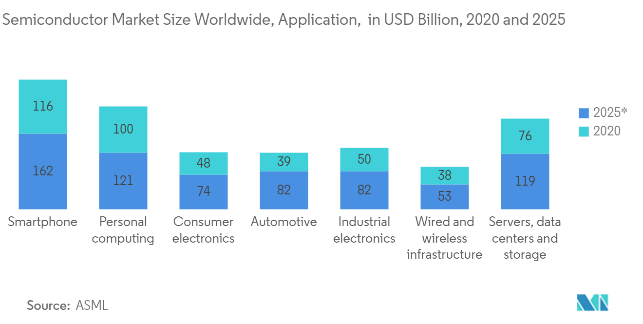
- Furthermore, semiconductor market growth along with development in high-density fan-out packaging solutions is expected to propel market growth over the forecast period. For instance, in July 2021, Changdian Technology, the world's premier combined circuit manufacturer and technology solution provider, revealed the official introduction of the entire line of very high-density fan-out packaging options for XDFOI chips, that are intended to deliver cost-effective, high-density connectivity, high-integration, and high-reliability solutions for chip heterogeneous integration.
- Advancements are also made in the fabrication method of manufacturing High-Density Fan-Out Wafer Level Packaging (FOWLP). Solutions are being developed to reduce chip size/height and lower production costs while improving reliability, energy efficiency, device speed, and multi-function integration. For instance, SPTS Technologies offers multiple plasma etch and deposition process technologies to leading semiconductor packaging companies for advanced packaging schemes such as that of high-density fan-out wafer-level packaging.
- Moreover, high-density fan-out (HDFO) packages can address these needs of miniaturization by fabrication capabilities of wafer-level processing coupled with its ability to create 3D structures using through-mold interconnects such as tall copper (Cu) pillars and through package vias (TPVs) and advanced flip chip packaging technologies.

Taiwan to Hold a Significant Share in the Market
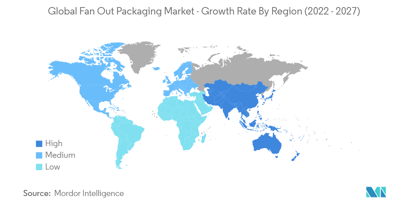
- Taiwan houses some of the major semiconductor manufacturing companies which are fueling the demand for advanced semiconductor packaging, especially in PLPs. According to a government think tank, Science and Technology International Strategy Center, Taiwan's output was expected to grow by 25.9% in 2021 to USD 147 billion.
- According to the Semiconductor Industry Association (SIA), Asia-Pacific generates more than 50% of revenue for global semiconductor sales; this, in turn, provides Taiwanese vendors with an opportunity to supply FOWLP for increased semiconductor applications.
- Most of the companies in the country are expanding their production capacity of Fan-out packaging, which is further expected to increase exports and help develop the local market. For instance, Intel, which recently announced its return to the foundry industry, will simultaneously invest USD 3.5 billion in New Mexico to construct a semiconductor packaging factory that will begin operations in the second half of 2022.
- Further, in June 2021, ASE, a pure semiconductor post-processing (OAST), started investing in advanced packaging facilities in response to the supply and demand shortage of semiconductors. It is accelerating the expansion by purchasing a large amount of semiconductor manufacturing equipment for WLP and PLP processes from HANMI Semiconductor.
- Also, the growing market for fifth-generation (5G) wireless communication and high-performance computing has enabled manufacturers to develop newer technologies. For instance, as a sole leader in the High-Density Fan-out segment, TSMC is planning to extend its FO-WLP segment into technologies like inFO-Antenna-in-Package (AiP) and inFO-on-Substrate (oS).


