2.5D and 3D Semiconductor Packaging Market Size

| Study Period | 2019 - 2029 |
| Market Size (2024) | USD 9.79 Billion |
| Market Size (2029) | USD 21.63 Billion |
| CAGR (2024 - 2029) | 17.20 % |
| Fastest Growing Market | Asia Pacific |
| Largest Market | Asia Pacific |
Major Players*Disclaimer: Major Players sorted in no particular order |
2.5D and 3D Semiconductor Packaging Market Analysis
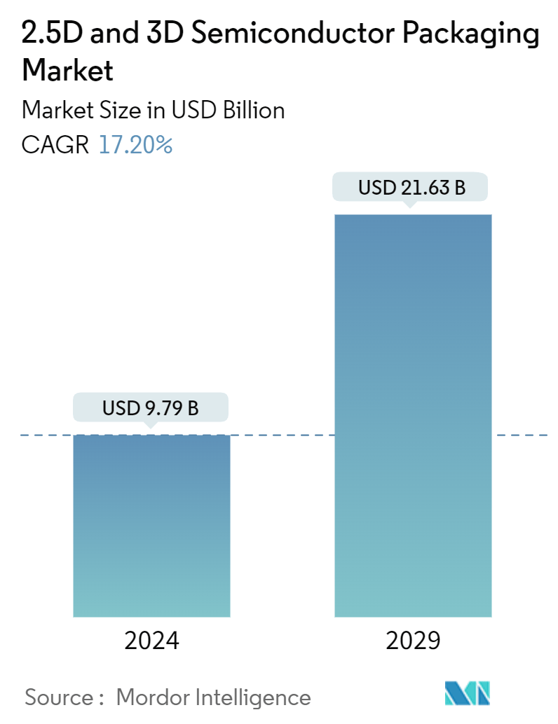
The 2.5D & 3D Semiconductor Packaging Market size is estimated at USD 9.79 billion in 2024, and is expected to reach USD 21.63 billion by 2029, growing at a CAGR of 17.20% during the forecast period (2024-2029).
2.5D and 3D are packaging methodologies that include multiple ICs inside the package. In a 2.5D structure, multiple active semiconductor chips are placed side-by-side on silicon interposers to achieve high die-to-die interconnect density. In a 3D structure, active chips are integrated by die stacking for the shortest interconnect and smallest package footprint. In recent years, 2.5D and 3D have gained momentum as ideal chipset integration platforms due to their merits in achieving extremely high packaging density and energy efficiency.
- High-performance computing, data center networking, and autonomous vehicles are pushing the adoption rates for the market studied and accelerating its technological evolution. The trend is to have more enormous computing resources at the cloud, edge computing, and device levels. The advancements in the market studied are also possible due to the growth in high-end performance applications and artificial intelligence (AI) in the telecom and infrastructure industry.
- Rising digitization, increasing trends of remote work and remote operations, and increasing consumer demand for electronics have sparked the need for advanced semiconductor devices that enable various new capabilities. As the demands for semiconductor devices intensify consistently, advanced packaging techniques provide the form factor and processing power required for today's digitized world.
- Information technology is revolutionizing the consumption pattern of modern consumers and products. Once composed solely of electrical and mechanical parts, products, especially electronic ones, are increasingly becoming complex systems that combine hardware, software, sensors, microprocessors, data storage, microprocessors, and connectivity in myriad ways, providing more functionalities to the resulting electronic devices.
- Significantly high initial investment is required in the design, development, and setting up of 2.5D/3D semiconductor packaging units as per the requirements of different industries. The major cost-driving processes of 3D semiconductor packaging include Through Silicon Via (TSV) creation yield loss, Wafer bumping, TSV reveals, Assembly yield, FOEL, BOEL, etc.
- According to the US Congressional Budget Office, defense spending in the United States was predicted to increase yearly until 2033. Defense outlays in the United States amounted to USD 746 billion in 2023. The forecast predicted an increase to USD 1.1 trillion in 2033. The increasing defense budgets globally are likely to offer lucrative opportunities for the growth of the market studied.
2.5D and 3D Semiconductor Packaging Market Trends
Communications and Telecom End-user Industry is Expected to Hold Significant Market Share
- Communications and telecom represent one of the fastest-growing segments of the market. The amount of data generated worldwide is increasing at a rapid pace. The explosion of data is fueled by many embedded devices that produce a small amount of data for each discrete transaction and add up to big data when clubbed together. Organizations collect data from various sources, including smart (IoT) devices, business transactions, industrial equipment, social media, etc.
- Organizations worldwide are looking to benefit from processing and acting upon data quickly. High-performance computing (HPC) has enabled businesses to scale computationally to build deep-learning algorithms that may take advantage of high volumes of data. As more data emerges, the need for more significant amounts of computing resources emerges, leading to greater adoption of HPC, which drives the market's growth. With the proliferation of high-performance computing, there is an escalating demand for semiconductor devices that deliver enhanced performance, lower latency, increased bandwidth, and power efficiency, creating significant demand for 2.5D and 3D packaging technologies.
- Communication base stations play a pivotal role in ensuring a robust communication ecosystem for mobile devices, including phones and smartphones. Given its high frequencies, 5G technology may efficiently manage vast data volumes at remarkable speeds, requiring a denser network of base stations. In contrast to 4G LTE, 5G base stations feature more transmitting antennas and components, leading to increased power consumption and heat generation.
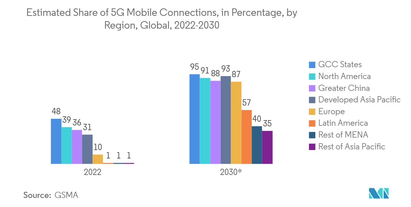
- According to the GSMA, in 2025, the share of 5G mobile connections of total connections in South Korea and Japan are anticipated to account for 73% and 68%, respectively. About 95% of mobile connections will be 5G by 2030 in GCC states and 93% in Asia. The increasing adoption of 5G smartphones and networks creates new market opportunities.
- The telecom industry continually advances data transmission speeds, driven by technologies such as 5G and its successors. These innovations demand robust infrastructure to manage the surge in data volumes. Companies may use 2.5D and 3D packaging to develop high-performance processors and network equipment, meeting the industry's escalating requirements.

China Expected to Witness Significant Growth
- Advancing technologies have contributed to the advancement and miniaturization of various consumer electronics, medical devices, telecom and communication devices, and automobiles by using compactly designed semiconductor chips, which would fuel the demand for the market in China.
- With the launch of 5G services in the country, smartphone demand has been increasing in China, which is likely to fuel the market's growth during the forecast period. The growth of connected devices, 5G-enabled smartphones, and the country's large manufacturing capabilities in the production of consumer electronic products are fueling the market's growth.
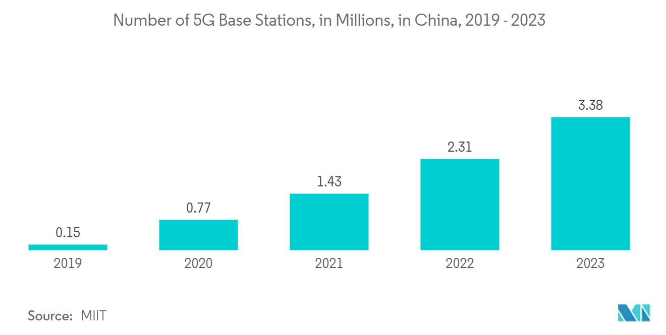
- According to MIIT, China's 5G infrastructure surged, boasting 3.38 million base stations by the close of 2023. Bolstered by substantial investments and aggressive deployment strategies, the nation achieved broad 5G coverage. Projections indicated a climb to over six million base stations by 2024. The rising execution of 5G in the region is also anticipated to boost the need for 5G-enabled devices, thereby increasing the demand for 2.5D and 3D semiconductor packaging in China.
- The growth of governmental investments and private players' product development to increase the efficiency of semiconductor components and support the increasing demand for energy-efficient electronic devices would support the market's growth.
- For instance, in August 2023, the National Natural Science Foundation of China (NSFC), a primary domestic funding source for basic research and frontier exploration, launched a new program to finance dozens of projects focused on chiplet technology. This would support the advancement in semiconductor packing and create an opportunity for market vendors operating in the country's 2.5D and 3D semiconductor packaging market.
- The Chinese market's large manufacturing capabilities, the existing industrial infrastructure, and the priority of the country's manufacturing of semiconductor devices would support the market's growth.
- For instance, in May 2024, China set up its third and largest state-backed semiconductor investment fund, worth USD 47.5 billion, as the country redoubled its efforts to build its domestic chip industry, which would support the demand for the 2.5D and 3D semiconductor packaging in the country due to its application in providing a protective enclosure for semiconductor devices.
- Therefore, the growth of governmental initiatives to strengthen the country's semiconductor ecosystem and the country's emergence as a global producer of the automotive and consumer electronic sectors would support the market's growth.

2.5D and 3D Semiconductor Packaging Industry Overview
The 2.5D & 3D Semiconductor market is semi-consolidated due to the presence of global players and small and medium-sized enterprises. Some major players in the market are ASE Group, Amkor Technology Inc., Intel Corporation, Samsung Electronics Co. Ltd, and Siliconware Precision Industries Co. Ltd (SPIL). Players in the market are adopting strategies such as acquisitions and partnerships to enhance their product offerings and gain sustainable competitive advantage.
- In April 2024, Samsung's AVP team received an order for advanced packaging for NVIDIA's AI chip, allowing for the future supply of high-bandwidth memory chips. The AVP team at Samsung Electronics may be responsible for providing interposer and 2.5D packaging technology for packaging NVIDIA's AI processors. However, the HBM and GPU chips used in these processors may come from other suppliers. 2.5D packaging technology allows for the horizontal integration of chips such as CPUs, GPUs, and HBMs on an interposer.
- In October 2023, Advanced Semiconductor Engineering Inc., a part of ASE Technology Holding Co. Ltd, introduced its Integrated Design Ecosystem (IDE). This collaborative design toolset aims to enhance advanced package architecture on its VIPack platform systematically. This new approach enables a smooth shift from a single-die SoC to multi-die disaggregated IP blocks like chiplets and memory for integration utilizing 2.5D or advanced fanout structures.
2.5D and 3D Semiconductor Packaging Market Leaders
-
ASE Group
-
Amkor Technology Inc.
-
Intel Corporation
-
Samsung Electronics Co. Ltd
-
Siliconware Precision Industries Co. Ltd (SPIL)
*Disclaimer: Major Players sorted in no particular order

2.5D and 3D Semiconductor Packaging Market News
- February 2024: Ansys and Intel Foundry partnered to offer Multiphysics signoff solutions for Intel's advanced 2.5D chip assembly technology. This technology utilizes EMIB technology to connect the die flexibly without using through-silicon via (TSVs). Ansys' precise simulation engines provide improved speeds, reduced power consumption, and increased reliability in sophisticated silicon systems for artificial intelligence (AI), high-performance computing, autonomous driving, and graphic processing.
- November 2023: Samsung Electronics was preparing to launch a new advanced 3D chip packaging technology called SAINT (Samsung Advanced Interconnection Technology) to compete with Taiwan Semiconductor Manufacturing Company's (TSMC) dominance in the market. The SAINT technology consists of three variants - SAINT D, SAINT L, and SAINT S - each aimed at improving the performance and integration of memory and processors for high-performance chips, particularly those utilized in AI applications.
2.5D & 3D Semiconductor Packaging Market Report - Table of Contents
1. INTRODUCTION
- 1.1 Study Assumptions and Market Definition
- 1.2 Scope of the Study
2. RESEARCH METHODOLOGY
3. EXECUTIVE SUMMARY
4. MARKET INSIGHTS
- 4.1 Market Overview
-
4.2 Industry Attractiveness - Porter's Five Forces Analysis
- 4.2.1 Bargaining Power of Suppliers
- 4.2.2 Bargaining Power of Buyers
- 4.2.3 Threat of New Entrants
- 4.2.4 Threat of Substitutes
- 4.2.5 Intensity of Competitive Rivalry
- 4.3 Value Chain Analysis
- 4.4 Analysis of Macroeconomic Trends on the Market
5. MARKET DYNAMICS
-
5.1 Market Drivers
- 5.1.1 Growing Consumption of Semiconductor Devices Across Several Industries
- 5.1.2 Increasing Demand for Compact, High Functionality Electronic Devices
-
5.2 Market Restraints
- 5.2.1 High Initial Investment and Increasing Complexity of Semiconductor IC Designs
-
5.3 Market Opportunities
- 5.3.1 Growing Adoption of High-end Computing, Servers, and Data Centers
6. MARKET SEGMENTATION
-
6.1 By Packaging Technology
- 6.1.1 3D
- 6.1.2 2.5D
- 6.1.3 3D Wafer-level chip-scale packaging (WLCSP) - Qualitative Analysis
-
6.2 By End-user Industry
- 6.2.1 Consumer Electronics
- 6.2.2 Medical Devices
- 6.2.3 Communications and Telecom
- 6.2.4 Automotive
- 6.2.5 Other End-user Industries
-
6.3 By Geography***
- 6.3.1 United States
- 6.3.2 China
- 6.3.3 Taiwan
- 6.3.4 South Korea
- 6.3.5 Japan
- 6.3.6 Europe
- 6.3.7 Latin America
- 6.3.8 Middle East & Africa
7. COMPETITIVE LANDSCAPE
-
7.1 Company Profiles*
- 7.1.1 ASE Group
- 7.1.2 Amkor Technology Inc.
- 7.1.3 Intel Corporation
- 7.1.4 Samsung Electronics Co. Ltd
- 7.1.5 Siliconware Precision Industries Co. Ltd (SPIL)
- 7.1.6 Powertech Technology Inc.
- 7.1.7 Jiangsu Changjiang Electronics Technology Co. Ltd
- 7.1.8 TSMC Limited
- 7.1.9 GlobalFoundries Inc.
- 7.1.10 Tezzaron Semiconductor Corporation.
8. INVESTMENT ANALYSIS
9. FUTURE OUTLOOK OF THE MARKET
** Subject To Availablity2.5D & 3D Semiconductor Packaging Industry Segmentation
2.5D/3D is a packaging methodology for having multiple ICs inside the package. In a 2.5D structure, two or more active semiconductor chips are positioned side-by-side on a silicon interposer to reach extremely high die-to-die interconnect density. In a 3D structure, active chips are combined by die stacking for the shortest interconnect and smallest package footprint. In recent years, 2.5D and 3D have gained momentum as ideal chipset integration platforms due to their merits in achieving extremely high packaging density and energy efficiency.
The 2.5D and 3D semiconductor packaging market is segmented by packaging technology (3D, 2.5D, 3D wafer-level chip-scale packaging (WLCSP) - Qualitative Analysis), end-user industry (consumer electronics, medical devices, communications and telecom, automotive, and other end-user industries), geography (United States, China, Taiwan, Korea, Japan, Europe, and the Rest of the World). The report offers the market size in value terms in USD for all the abovementioned segments.
| By Packaging Technology | 3D |
| 2.5D | |
| 3D Wafer-level chip-scale packaging (WLCSP) - Qualitative Analysis | |
| By End-user Industry | Consumer Electronics |
| Medical Devices | |
| Communications and Telecom | |
| Automotive | |
| Other End-user Industries | |
| By Geography*** | United States |
| China | |
| Taiwan | |
| South Korea | |
| Japan | |
| Europe | |
| Latin America | |
| Middle East & Africa |
2.5D & 3D Semiconductor Packaging Market Research FAQs
How big is the 2.5D & 3D Semiconductor Packaging Market?
The 2.5D & 3D Semiconductor Packaging Market size is expected to reach USD 9.79 billion in 2024 and grow at a CAGR of 17.20% to reach USD 21.63 billion by 2029.
What is the current 2.5D & 3D Semiconductor Packaging Market size?
In 2024, the 2.5D & 3D Semiconductor Packaging Market size is expected to reach USD 9.79 billion.
Who are the key players in 2.5D & 3D Semiconductor Packaging Market?
ASE Group, Amkor Technology Inc., Intel Corporation, Samsung Electronics Co. Ltd and Siliconware Precision Industries Co. Ltd (SPIL) are the major companies operating in the 2.5D & 3D Semiconductor Packaging Market.
Which is the fastest growing region in 2.5D & 3D Semiconductor Packaging Market?
Asia Pacific is estimated to grow at the highest CAGR over the forecast period (2024-2029).
Which region has the biggest share in 2.5D & 3D Semiconductor Packaging Market?
In 2024, the Asia Pacific accounts for the largest market share in 2.5D & 3D Semiconductor Packaging Market.
What years does this 2.5D & 3D Semiconductor Packaging Market cover, and what was the market size in 2023?
In 2023, the 2.5D & 3D Semiconductor Packaging Market size was estimated at USD 8.11 billion. The report covers the 2.5D & 3D Semiconductor Packaging Market historical market size for years: 2019, 2020, 2021, 2022 and 2023. The report also forecasts the 2.5D & 3D Semiconductor Packaging Market size for years: 2024, 2025, 2026, 2027, 2028 and 2029.
2.5D & 3D Semiconductor Packaging Industry Report
Statistics for the 2024 2.5D & 3D Semiconductor Packaging market share, size and revenue growth rate, created by Mordor Intelligence™ Industry Reports. 2.5D & 3D Semiconductor Packaging analysis includes a market forecast outlook to 2029 and historical overview. Get a sample of this industry analysis as a free report PDF download.


