Market Size of 2.5D & 3D Semiconductor Packaging Industry

| Study Period | 2019 - 2029 |
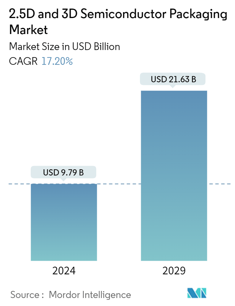
| Market Size (2024) | USD 9.79 Billion |
| Market Size (2029) | USD 21.63 Billion |
| CAGR (2024 - 2029) | 17.20 % |
| Fastest Growing Market | Asia Pacific |
| Largest Market | Asia Pacific |
Major Players*Disclaimer: Major Players sorted in no particular order |
2.5D and 3D Semiconductor Packaging Market Analysis
The 2.5D & 3D Semiconductor Packaging Market size is estimated at USD 9.79 billion in 2024, and is expected to reach USD 21.63 billion by 2029, growing at a CAGR of 17.20% during the forecast period (2024-2029).
2.5D and 3D are packaging methodologies that include multiple ICs inside the package. In a 2.5D structure, multiple active semiconductor chips are placed side-by-side on silicon interposers to achieve high die-to-die interconnect density. In a 3D structure, active chips are integrated by die stacking for the shortest interconnect and smallest package footprint. In recent years, 2.5D and 3D have gained momentum as ideal chipset integration platforms due to their merits in achieving extremely high packaging density and energy efficiency.
- High-performance computing, data center networking, and autonomous vehicles are pushing the adoption rates for the market studied and accelerating its technological evolution. The trend is to have more enormous computing resources at the cloud, edge computing, and device levels. The advancements in the market studied are also possible due to the growth in high-end performance applications and artificial intelligence (AI) in the telecom and infrastructure industry.
- Rising digitization, increasing trends of remote work and remote operations, and increasing consumer demand for electronics have sparked the need for advanced semiconductor devices that enable various new capabilities. As the demands for semiconductor devices intensify consistently, advanced packaging techniques provide the form factor and processing power required for today's digitized world.
- Information technology is revolutionizing the consumption pattern of modern consumers and products. Once composed solely of electrical and mechanical parts, products, especially electronic ones, are increasingly becoming complex systems that combine hardware, software, sensors, microprocessors, data storage, microprocessors, and connectivity in myriad ways, providing more functionalities to the resulting electronic devices.
- Significantly high initial investment is required in the design, development, and setting up of 2.5D/3D semiconductor packaging units as per the requirements of different industries. The major cost-driving processes of 3D semiconductor packaging include Through Silicon Via (TSV) creation yield loss, Wafer bumping, TSV reveals, Assembly yield, FOEL, BOEL, etc.
- According to the US Congressional Budget Office, defense spending in the United States was predicted to increase yearly until 2033. Defense outlays in the United States amounted to USD 746 billion in 2023. The forecast predicted an increase to USD 1.1 trillion in 2033. The increasing defense budgets globally are likely to offer lucrative opportunities for the growth of the market studied.
2.5D & 3D Semiconductor Packaging Industry Segmentation
2.5D/3D is a packaging methodology for having multiple ICs inside the package. In a 2.5D structure, two or more active semiconductor chips are positioned side-by-side on a silicon interposer to reach extremely high die-to-die interconnect density. In a 3D structure, active chips are combined by die stacking for the shortest interconnect and smallest package footprint. In recent years, 2.5D and 3D have gained momentum as ideal chipset integration platforms due to their merits in achieving extremely high packaging density and energy efficiency.
The 2.5D and 3D semiconductor packaging market is segmented by packaging technology (3D, 2.5D, 3D wafer-level chip-scale packaging (WLCSP) - Qualitative Analysis), end-user industry (consumer electronics, medical devices, communications and telecom, automotive, and other end-user industries), geography (United States, China, Taiwan, Korea, Japan, Europe, and the Rest of the World). The report offers the market size in value terms in USD for all the abovementioned segments.
| By Packaging Technology | |
| 3D | |
| 2.5D | |
| 3D Wafer-level chip-scale packaging (WLCSP) - Qualitative Analysis |
| By End-user Industry | |
| Consumer Electronics | |
| Medical Devices | |
| Communications and Telecom | |
| Automotive | |
| Other End-user Industries |
| By Geography*** | |
| United States | |
| China | |
| Taiwan | |
| South Korea | |
| Japan | |
| Europe | |
| Latin America | |
| Middle East & Africa |
2.5D & 3D Semiconductor Packaging Market Size Summary
The 2.5D and 3D semiconductor packaging market is experiencing significant growth, driven by the increasing demand for high-performance computing, data center networking, and autonomous vehicles. These packaging methodologies, which involve integrating multiple semiconductor chips within a single package, are gaining traction due to their ability to achieve high packaging density and energy efficiency. The market is further propelled by advancements in artificial intelligence and the telecom infrastructure industry, as well as the rising digitization and consumer demand for advanced electronic devices. The need for compact and efficient semiconductor devices is becoming more critical as products evolve into complex systems that combine hardware, software, and connectivity features.
The market landscape is characterized by a semi-consolidated structure with major players like ASE Group, Amkor Technology Inc., Intel Corporation, Samsung Electronics Co. Ltd, and Siliconware Precision Industries Co. Ltd (SPIL) leading the charge. These companies are actively engaging in strategic partnerships and acquisitions to enhance their product offerings and maintain a competitive edge. The increasing adoption of 5G technology and the subsequent demand for 5G-enabled devices are creating new opportunities, particularly in regions like China, where substantial investments in 5G infrastructure are underway. Additionally, governmental initiatives and private sector investments in semiconductor technology are expected to bolster market growth, supporting the development of energy-efficient and high-performance semiconductor components.
2.5D & 3D Semiconductor Packaging Market Size - Table of Contents
-
1. MARKET INSIGHTS
-
1.1 Market Overview
-
1.2 Industry Attractiveness - Porter's Five Forces Analysis
-
1.2.1 Bargaining Power of Suppliers
-
1.2.2 Bargaining Power of Buyers
-
1.2.3 Threat of New Entrants
-
1.2.4 Threat of Substitutes
-
1.2.5 Intensity of Competitive Rivalry
-
-
1.3 Value Chain Analysis
-
1.4 Analysis of Macroeconomic Trends on the Market
-
-
2. MARKET SEGMENTATION
-
2.1 By Packaging Technology
-
2.1.1 3D
-
2.1.2 2.5D
-
2.1.3 3D Wafer-level chip-scale packaging (WLCSP) - Qualitative Analysis
-
-
2.2 By End-user Industry
-
2.2.1 Consumer Electronics
-
2.2.2 Medical Devices
-
2.2.3 Communications and Telecom
-
2.2.4 Automotive
-
2.2.5 Other End-user Industries
-
-
2.3 By Geography***
-
2.3.1 United States
-
2.3.2 China
-
2.3.3 Taiwan
-
2.3.4 South Korea
-
2.3.5 Japan
-
2.3.6 Europe
-
2.3.7 Latin America
-
2.3.8 Middle East & Africa
-
-
2.5D & 3D Semiconductor Packaging Market Size FAQs
How big is the 2.5D & 3D Semiconductor Packaging Market?
The 2.5D & 3D Semiconductor Packaging Market size is expected to reach USD 9.79 billion in 2024 and grow at a CAGR of 17.20% to reach USD 21.63 billion by 2029.
What is the current 2.5D & 3D Semiconductor Packaging Market size?
In 2024, the 2.5D & 3D Semiconductor Packaging Market size is expected to reach USD 9.79 billion.


