Market Size of Semiconductor Lithography Equipment Industry

| Study Period | 2019 - 2029 |
| Market Size (2024) | USD 26.48 Billion |
| Market Size (2029) | USD 37.81 Billion |
| CAGR (2024 - 2029) | 7.38 % |
| Fastest Growing Market | Asia Pacific |
| Largest Market | Asia Pacific |
Major Players*Disclaimer: Major Players sorted in no particular order |
Semiconductor Lithography Equipment Market Analysis
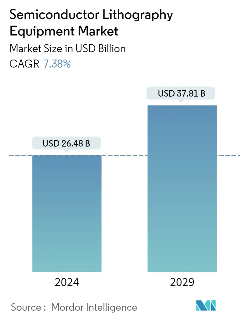
The Semiconductor Lithography Equipment Market size is estimated at USD 26.48 billion in 2024, and is expected to reach USD 37.81 billion by 2029, growing at a CAGR of 7.38% during the forecast period (2024-2029).
- The semiconductor lithography equipment market is expected to grow with the growing manufacturing of semiconductor devices that are widely used in nearly all sectors including consumer electronics, automotive, and many others. Smart device adoption is increasing and is expected to grow as 5G connections and adoption spread over the globe. As per GSMA, 5G mobile broadband connections are expected to reach 1,100 million by 2025, with the 5G rollout expected to cover 34 percent of the world's population by 2025.
- More than 50 percent of the semiconductor FAB (fabrication) cost is due to equipment and tools. One piece of equipment that drives the semiconductor fabrication process forward is lithography. There are several aspects of semiconductor fabrication that has driven by lithography equipment. Yield and defect are two such examples from the technical point of view. It is the primary reason why semiconductor fabrication focuses a lot on which type of lithography technology to deploy.
- With the rising complexity in semiconductor products, the types of defects are also getting complex. However, lithography equipment is supposed to handle the complex process. With semiconductor manufacturers focusing on next-gen advanced technology nodes, the importance of error-free lithography equipment is significantly increasing further.
- Moreover, manufacturing businesses are are lately growing at a signficant rate with the advent of 5G and emergence of IoT connected devices, which is anticipated to facilitate the connection required for various Industry 4.0 applications, such as wireless control. This is especially essential for mobile tools, machines, and robots that can aid market growth during the forecast period.
- Several industry players are focusing on offering new lithography systems to serve a wide range of applications. For instance, in March 2022, Nikon Corporation announced to launch new Gen 8 plate FPD lithography system to support the production of various high-definition panels for value-added premium displays, such as high-end monitors, large TVs, and smart devices.
- The semiconductor industry is considered as one of the most complex industries, not only owing to the presence of more than 500 processing steps involved in the manufacturing and inspection and various products but also due to the harsh environment it goes through, e.g., the volatile electronic market and the unpredictable demand. Therefore, depending on the intricacy of the manufacturing process, there are about 1,400 process steps in the complete manufacturing and inspection of semiconductor wafers alone. Such a complex process poses a notable hurdle to the market's growth.
Semiconductor Lithography Equipment Industry Segmentation
A semiconductor lithography system at its core is a projection system. This equipment is used to draw highly complex circuit patterns on a photomask that is usually made of large glass plates. To do this, these types of equipment reduce the size of the circuit pattern using ultra-high-performance lenses and expose them onto a silicon substrate called a wafer. The lithography equipment is broadly categorized into dry and immersion types, and the EUV lithography machine is considered the most advanced.
The market for semiconductor lithography equipment was evaluated by analyzing separate market sizes for deep ultraviolet lithography (DUV) (ArFi, ArF dry, KrF, i-line) and extreme ultraviolet lithography (EUV) for different applications, including advanced packaging, MEMS devices, and LED devices in multiple geographies, including North America, Europe, Asia-Pacific, and the Rest of the World. The study also examines the impact of macroeconomic trends on the market and impacted segments. The study also discusses the drivers and restraints likely to influence the market's evolution in the near future. The market sizes and forecasts are provided in terms of USD value for all the above segments.
| Type | |
| Deep Ultraviolet Lithography (DUV) | |
| Extreme Ultraviolet Lithography (EUV) |
| Application | |
| Advanced Packaging | |
| MEMS Devices | |
| LED Devices |
| Geography | |
| North America | |
| Europe | |
| Asia | |
| Australia and New Zealand | |
| Latin America | |
| Middle East and Africa |
Semiconductor Lithography Equipment Market Size Summary
The semiconductor lithography equipment market is poised for significant growth, driven by the increasing demand for semiconductor devices across various sectors such as consumer electronics and automotive. The proliferation of smart devices, fueled by the global rollout of 5G technology, is a key factor propelling this market expansion. Lithography equipment plays a crucial role in semiconductor fabrication, impacting yield and defect rates, which are vital for the production of complex semiconductor products. As manufacturers focus on advanced technology nodes, the demand for error-free lithography equipment becomes even more critical. The rise of IoT and Industry 4.0 applications further stimulates market growth, as these technologies require sophisticated semiconductor solutions.
The market landscape is characterized by a concentration of major players like ASML, Nikon, and Veeco, who dominate the market share with their advanced lithography systems. Innovations such as Deep UV lithography are driving the miniaturization trend, enabling the production of more efficient microchips at reduced costs. The United States, with its robust R&D capabilities and significant investments, is a key player in the semiconductor industry, further bolstered by government initiatives to enhance domestic manufacturing. The market's growth is supported by strategic collaborations and technological advancements, although it faces challenges due to the complex and volatile nature of the semiconductor manufacturing process.
Semiconductor Lithography Equipment Market Size - Table of Contents
-
1. MARKET INSIGHTS
-
1.1 Market Overview
-
1.2 Industry Attractiveness - Porter's Five Forces Analysis
-
1.2.1 Bargaining Power of Suppliers
-
1.2.2 Bargaining Power of Buyers
-
1.2.3 Threat of New Entrants
-
1.2.4 Threat of Substitute Products
-
1.2.5 Intensity of Competitive Rivalry
-
-
1.3 Semiconductor Lithography Equipment Technology Roadmap
-
1.4 The impact of macroeconomic trends on the Market
-
-
2. MARKET SEGMENTATION
-
2.1 Type
-
2.1.1 Deep Ultraviolet Lithography (DUV)
-
2.1.2 Extreme Ultraviolet Lithography (EUV)
-
-
2.2 Application
-
2.2.1 Advanced Packaging
-
2.2.2 MEMS Devices
-
2.2.3 LED Devices
-
-
2.3 Geography
-
2.3.1 North America
-
2.3.2 Europe
-
2.3.3 Asia
-
2.3.4 Australia and New Zealand
-
2.3.5 Latin America
-
2.3.6 Middle East and Africa
-
-
Semiconductor Lithography Equipment Market Size FAQs
How big is the Semiconductor Lithography Equipment Market?
The Semiconductor Lithography Equipment Market size is expected to reach USD 26.48 billion in 2024 and grow at a CAGR of 7.38% to reach USD 37.81 billion by 2029.
What is the current Semiconductor Lithography Equipment Market size?
In 2024, the Semiconductor Lithography Equipment Market size is expected to reach USD 26.48 billion.


