Market Size of Semiconductor Packaging Industry

| Study Period | 2019 - 2029 |
| Base Year For Estimation | 2023 |
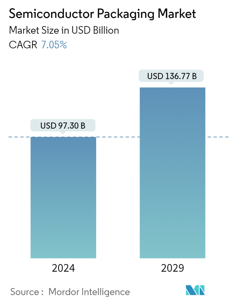
| Market Size (2024) | USD 97.30 Billion |
| Market Size (2029) | USD 136.77 Billion |
| CAGR (2024 - 2029) | 7.05 % |
| Market Concentration | Medium |
Major Players*Disclaimer: Major Players sorted in no particular order |
Semiconductor Packaging Market Analysis
The Semiconductor Packaging Market size is estimated at USD 97.30 billion in 2024, and is expected to reach USD 136.77 billion by 2029, growing at a CAGR of 7.05% during the forecast period (2024-2029).
Semiconductor packaging refers to a casing that contains one or more discrete semiconductor devices or integrated circuits made up of plastic, ceramic, metal, or glass casing. Packaging is crucial for protecting an electronic system from radio frequency noise emission, electrostatic discharge, mechanical damage, and cooling.
High-performance computing, data center networking, and autonomous vehicles are pushing the adoption rates for the market studied and accelerating its technological evolution. The trend is to have more enormous computing resources at the cloud, edge computing, and device levels. The advancements in the market studied are also possible due to the growth in high-end performance applications and artificial intelligence (AI) in the telecom and infrastructure industry.
As the front-end node becomes smaller, design cost becomes increasingly important. Advanced packaging (AP) solutions aid in solving these problems by reducing the cost while enhancing system performance and offering lower latency, increased bandwidth, and power efficiency.
The increasing digitization of the workplace, the emergence of remote working and remote operation trends, and the growing consumer preference for electronics have increased the demand for semiconductor devices capable of unlocking a wide range of new opportunities. As the growth of semiconductor devices continues to accelerate, advanced packaging technologies provide the size and processing power necessary for the digitized era.
Global governments are increasingly supporting the semiconductor industry by lowering barriers and ramping up production, research, and development subsidies. For instance, South Korea committed a staggering USD 456 billion in private investments to construct the world's largest chip center, underlining its ambitions for industry dominance.
In tandem with this, the South Korean government rolled out an extensive support initiative for its semiconductor industry, valued at KRW 26 trillion (approximately USD 19.1 billion). This program spans financial aid, infrastructure development, R&D, and targeted assistance for its SMEs. Just outside Seoul, South Korea is currently in the works of creating a "mega chip cluster," which is projected to become the largest semiconductor hub globally and a key driver in creating numerous new employment opportunities.
A significantly high initial investment is required in designing, developing, and setting up semiconductor packaging units as per the requirements of different industries such as automotive, consumer electronics, healthcare, IT and telecommunication, and aerospace and defense. This can restrict the growth of the semiconductor packaging market.
Moreover, the defense budgets of various countries are significantly influenced by major macroeconomic factors such as inflation, economic growth, government spending priorities, and global trade and geopolitical dynamics.
In March 2023, President Joe Biden proposed the largest peacetime US defense budget, totaling USD 886 billion. This budget notably included a 5.2% pay raise for troops and marked the highest-ever allocation for research and development. The backdrop of Russia's actions in Ukraine further underscored the need for increased spending on munitions.
As per the US Congressional Budget Office, the United States is set to witness a consistent rise in defense spending, with projections extending until 2033. In 2023, the United States spent USD 746 billion on defense, with forecasts indicating a climb to USD 1.1 trillion by 2033.
Semiconductor Packaging Industry Segmentation
Semiconductor packaging refers to a casing that contains one or more discrete semiconductor devices or integrated circuits made of plastic, ceramic, metal, or glass casing. Packaging protects an electronic system from radio frequency noise emission, electrostatic discharge, mechanical damage, and cooling. The rise in the semiconductor industry worldwide is one of the major factors driving the growth of the semiconductor packaging market. The continuous advancements in terms of integration, energy efficiency, and product characteristics because of the growing demand across various end-user verticals of the industry and the use of packaging for improving the performance, reliability, and cost-effectiveness of electronic systems accelerate the market’s growth.
The report tracks the sales of semiconductor packaging globally to evaluate the market revenue for the global advanced packaging and traditional packaging market. Different advanced packaging platforms are considered in the report, including flip-chip, fan-in, embedded die, 3D stacking, and fan-out packaging, which are used in multiple end-user applications like consumer electronics, medical devices, communication and telecom, and automotive. The competitive landscape has been taken to calculate packaging penetration and how players involve themselves in organic and inorganic growth strategies. These companies are innovating their products to increase their market share and profitability. Furthermore, the report focuses on analyzing macroeconomic factors in the market.
The semiconductor packaging market is segmented by packaging platform (advanced packaging [flip chip, SIP, 2.5D/3D, embedded die, fan-in wafer level packaging (FI-WLP), and fan-out wafer level packaging (FO-WLP)] and traditional packaging), end-user industry (consumer electronics, aerospace and defense, medical devices, communications and telecom, automotive, and energy and lighting), and geography (United States, China, Taiwan, Korea, Japan, and Europe). The report offers market sizes and forecasts in terms of value (USD) for all these segments.
| By Packaging Platform | ||||||||
| ||||||||
| Traditional Packaging |
| By End-user Industry | |
| Consumer Electronics | |
| Aerospace and Defense | |
| Medical Devices | |
| Communications and Telecom | |
| Automotive Industry | |
| Energy and Lighting |
| By Geography*** | |
| United States | |
| China | |
| Taiwan | |
| South Korea | |
| Japan | |
| Europe | |
| Latin America | |
| Middle East and Africa |
Semiconductor Packaging Market Size Summary
The semiconductor packaging market is poised for significant growth, driven by the increasing demand for advanced packaging solutions across various industries. This market is essential for protecting semiconductor devices and integrated circuits from environmental factors and enhancing their performance. The rise of high-performance computing, data center networking, and autonomous vehicles is accelerating the adoption of semiconductor packaging technologies. Additionally, the proliferation of artificial intelligence and advanced telecommunications, particularly with the rollout of 5G, is further propelling market expansion. The market is also benefiting from substantial government support and investments, particularly in regions like South Korea and Taiwan, where initiatives are underway to bolster semiconductor manufacturing capabilities and infrastructure.
The market landscape is characterized by a semi-consolidated structure with key players such as ASE Technology Holding Co. Ltd, Amkor Technology, and TSMC leading the charge. These companies are actively engaging in strategic partnerships and technological innovations to maintain a competitive edge. The demand for semiconductor packaging is further fueled by the growing digitization of workplaces, the expansion of cloud technologies, and the increasing penetration of data centers. However, the market faces challenges, including the high initial investment required for setting up packaging units and the influence of macroeconomic factors on defense budgets. Despite these challenges, the market is expected to continue its upward trajectory, supported by ongoing advancements in packaging technologies and the expanding application of semiconductors across various sectors.
Semiconductor Packaging Market Size - Table of Contents
-
1. MARKET INSIGHTS
-
1.1 Market Overview
-
1.2 Industry Attractiveness - Porter's Five Forces Analysis
-
1.2.1 Bargaining Power of Suppliers
-
1.2.2 Bargaining Power of Buyers
-
1.2.3 Threat of New Entrants
-
1.2.4 Threat of Substitutes
-
1.2.5 Intensity of Competitive Rivalry
-
-
1.3 Industry Value Chain Analysis
-
1.4 Impact of COVID-19 Aftereffects and Other Macroeconomic Factors on the Market
-
-
2. MARKET SEGMENTATION
-
2.1 By Packaging Platform
-
2.1.1 Advanced Packaging
-
2.1.1.1 Flip Chip
-
2.1.1.2 SIP
-
2.1.1.3 2.5D/3D
-
2.1.1.4 Embedded Die
-
2.1.1.5 Fan-in Wafer Level Packaging (FI-WLP)
-
2.1.1.6 Fan-out Wafer Level Packaging (FO-WLP)
-
-
2.1.2 Traditional Packaging
-
-
2.2 By End-user Industry
-
2.2.1 Consumer Electronics
-
2.2.2 Aerospace and Defense
-
2.2.3 Medical Devices
-
2.2.4 Communications and Telecom
-
2.2.5 Automotive Industry
-
2.2.6 Energy and Lighting
-
-
2.3 By Geography***
-
2.3.1 United States
-
2.3.2 China
-
2.3.3 Taiwan
-
2.3.4 South Korea
-
2.3.5 Japan
-
2.3.6 Europe
-
2.3.7 Latin America
-
2.3.8 Middle East and Africa
-
-
Semiconductor Packaging Market Size FAQs
How big is the Semiconductor Packaging Market?
The Semiconductor Packaging Market size is expected to reach USD 97.30 billion in 2024 and grow at a CAGR of 7.05% to reach USD 136.77 billion by 2029.
What is the current Semiconductor Packaging Market size?
In 2024, the Semiconductor Packaging Market size is expected to reach USD 97.30 billion.


