Thin Wafer Processing & Dicing Equipment Market Size
| Study Period | 2019 - 2029 |
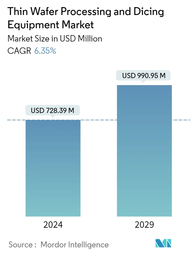
| Market Size (2024) | USD 728.39 Million |
| Market Size (2029) | USD 990.95 Million |
| CAGR (2024 - 2029) | 6.35 % |
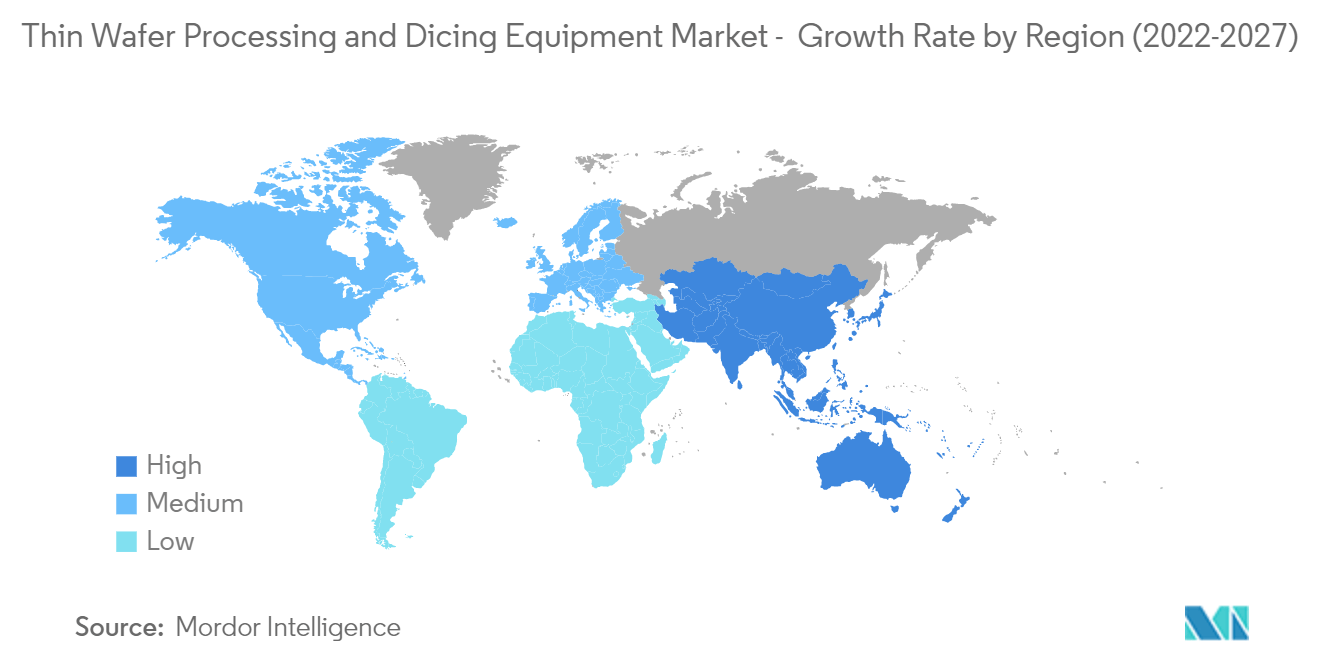
| Fastest Growing Market | Asia Pacific |
| Largest Market | Asia Pacific |
Major Players
*Disclaimer: Major Players sorted in no particular order |
Thin Wafer Processing & Dicing Equipment Market Analysis
The Thin Wafer Processing and Dicing Equipment Market size is estimated at USD 728.39 million in 2024, and is expected to reach USD 990.95 million by 2029, growing at a CAGR of 6.35% during the forecast period (2024-2029).
The increasing efforts to make electronic packaging highly resourceful due to the enormous demand for electronic components owing to amplified usage have made electronic packaging useful in a myriad of applications. These factors are driving the growth of the semiconductor and IC packaging market.
- One of the major factors expected to boost the demand for thin wafer processing and dicing equipment in the coming years is the growing demand for three-dimensional integrated circuits, which are widely used in miniature semiconductor devices such as memory cards, smartphones, and smart cards, and various computing devices. Three-dimensional circuits are becoming more popular in multiple space-constrained applications, such as portable consumer electronics, sensors, MEMS, and industrial products because they improve overall product performance in terms of speed, durability, low power consumption, and lightweight memory.
- The expanding use of server and data center systems across various enterprises and industries, due to the widespread availability of low-cost cloud computing solutions, is likely to fuel demand for logic devices like microprocessors and digital signal processors. In addition, as the number of IoT-enabled linked devices grows, the utilization of microprocessors also increases. Thin wafers are increasingly employed in these devices to enable effective temperature management and enhance performance. All of these reasons are assisting in expanding the logic device market.
- Silicon wafers have long been used as a fabrication platform in microelectronics and MEMS. The silicon-on-insulator substrate is a unique variation of the standard silicon wafer. Two silicon wafers are glued together using a bond layer of silicon dioxide with a thickness of about 1-2 m to make these wafers. One silicon wafer gets flattened down to 10-50 m in thickness. The application will determine the exact thickness of the coating.
- The cost of building state-of-the-art thin wafer foundries has increased exponentially, which puts pressure on the industry. This is where the number of semiconductor manufacturers was consolidated in recent times. Performance boosts are slowing down, making specialized thin wafers increasingly attractive. The design decisions that enable thin wafers to be universal may be sub-optimal for some computing tasks.
- Due to the global slowdown in demand in the industrial and automotive electronics sectors that the COVID-19 pandemic has worsened, manufacturers operating in the market have registered a decline in orders for Thin Wafer semiconductors.
Thin Wafer Processing & Dicing Equipment Market Trends
This section covers the major market trends shaping the Thin Wafer Processing & Dicing Equipment Market according to our research experts:
Increasing Need for Miniaturization of Semiconductors to Drive the Market
- Due to increasing demand for compact electronic devices in segments such as consumer electronics, healthcare, and automotive, semiconductor IC manufacturers are forced to reduce the size of ICs. It has, therefore, given rise to miniaturization in the market, which is expected to experience a surge in its demand during the forecast period.
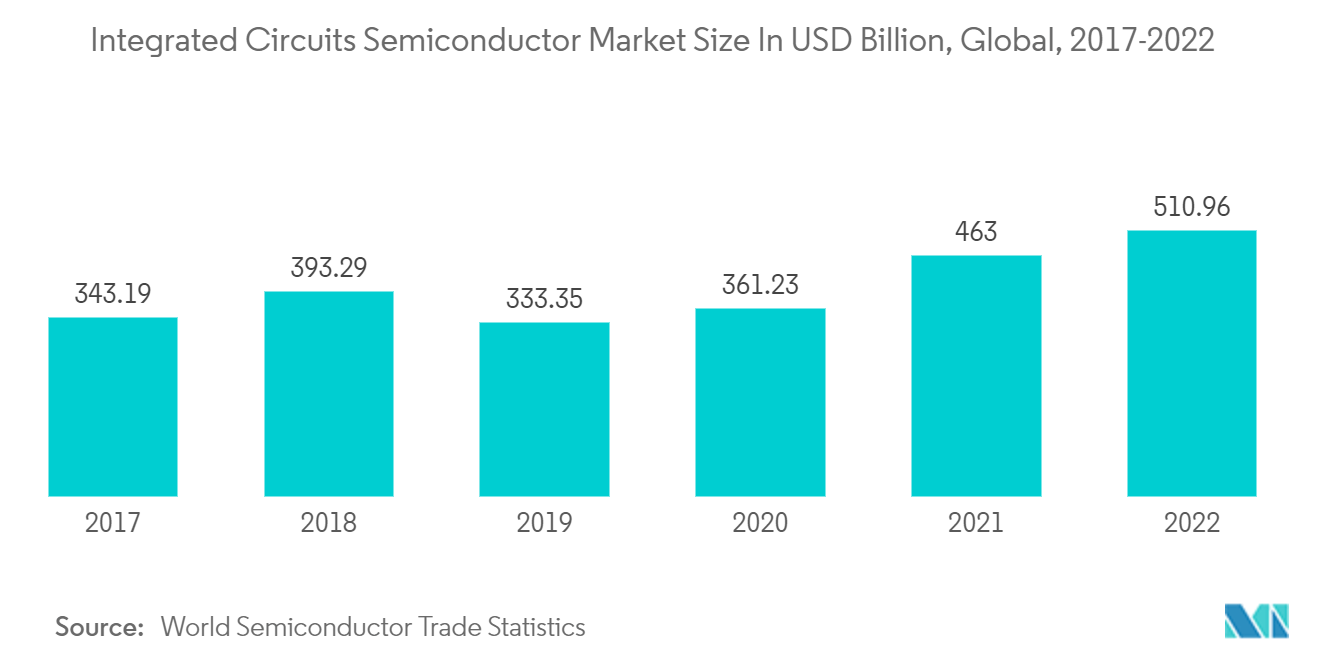
- Across geographies, the fabless business model is the major contributor to the prominent position of various Asian countries in semiconductor sales across the world. Fabless firms typically outsource fabrication to pure-play foundries and outsourced assembly and test (OSAT) firms. According to the report published by the Semiconductor Industry Association (SIA), in 2021, the dominance of the United States has decreased severely from 1990 and accounted for only 12% of the semiconductor manufacturing capacity. The rise of East Asia, especially China, is credited to various incentives and subsidies offered by the governments of various countries.
- According to Fujifilm, the miniaturization of semiconductor devices continues as the increasing use of AI, IoT, next-generation communication standard '5G', and the advancement of autonomous driving technology are expected to increase further demand and performance boost for semiconductors. The factors mentioned above have led to the rise in demand for small and lightweight consumer devices that rely on 3D circuit architecture built onto ultra-thin silicon wafers in order to perform at peak capacity.
- These wafers are extremely thin and flat. At the same time, miniaturization has resulted in the need to integrate several features on a single chip. Due to the large-sized wafers (with a diameter of up to 12 inches), there is a new trend in wafer technology.
- In May 2021, with the invention of the first chip using 2 nanometers (nm) nanosheet technology, IBM announced a breakthrough in semiconductor design and process. Semiconductors are used in a wide range of applications, including computers, appliances, communication devices, transportation systems, and critical infrastructure. Chip performance and energy efficiency are in high demand, particularly in the age of hybrid cloud, AI, and the Internet of Things. IBM's innovative 2 nm chip technology contributes to advancing the semiconductor industry's state-of-the-art, answering this expanding demand. It's expected to deliver 45% better performance and 75% lower energy consumption than today's most advanced 7 nm node chips.
Asia Pacific to Hold the Largest Market Share
- The Asia Pacific is the largest and fastest-growing semiconductor market in the world. Significant demand for smartphones and other consumer electronics devices from countries such as China, the Republic of Korea, and Singapore, are encouraging many vendors to set up production establishments in the region.
- China's various players in the market are focusing on expanding business through acquisitions and mergers. For instance, in August 2021, Wingtech acquired Newport Wafer Fab for around EUR 63 million through a Dutch subsidiary called Nexperia. The deal was announced in July, confirming the terms of the agreement, according to a Wingtech statement filed with the Shanghai Stock Exchange. Wingtech is a listed manufacturer that assembles smartphones and other home appliances.
- Japan occupies an essential position in the semiconductor industry as it is home to several major manufacturers and the electronics industry. The government is expected to begin an investigation to assess the potential for bringing major chip makers into the country. Meanwhile, Japan-based organizations are considered the significant suppliers of most of the critical materials consumed in semiconductor manufacturing and packaging. For Japanese-based suppliers, Japanese exchange rates and high production costs make materials more expensive and open up opportunities for other suppliers for low-end applications.
- In Australia, the growing electronics manufacturing sector and the increasing adoption of advanced devices among various end-user industries are influencing the market growth. The sales of televisions and smartphones have primarily driven the growth in consumer electronics.
- In October 2021, in Australia, India, the United States, and Japan, the Quad Alliance also launched a semiconductor supply chain initiative aimed at capacity mapping, vulnerability identification, and enhanced supply chain security for semiconductors and their critical components. Together with NSW's Semiconductor Sector Service Bureau, these are the proper steps to establish Australia as a player in the Asia Pacific region and secure its position in the global semiconductor supply chain.
- Currently, India's semiconductor demand is majorly met by imports. Therefore, it was necessary to incentivize the value chain to make India economically independent and technologically leading. The government envisioned a comprehensive program in December 2021 to develop India's semiconductor and display manufacturing ecosystem with a budget of over INR 76,000 crores. Financial support efforts under the new program amounted to INR 230,000, covering the entire electrical device supply chain and more.
- The growth trajectory of fully-autonomous automobiles is heavily influenced by factors in Asia-Pacific, including technology advancements, consumer willingness to accept fully-automated vehicles, pricing, and suppliers' and OEMs' capacity to address significant concerns about vehicles safety. According to these factors, the automotive and semiconductor industries are always concentrating on enhancing technologies, negotiating raw material prices, and finally combining cars with reliable technology.
Thin Wafer Processing & Dicing Equipment Industry Overview
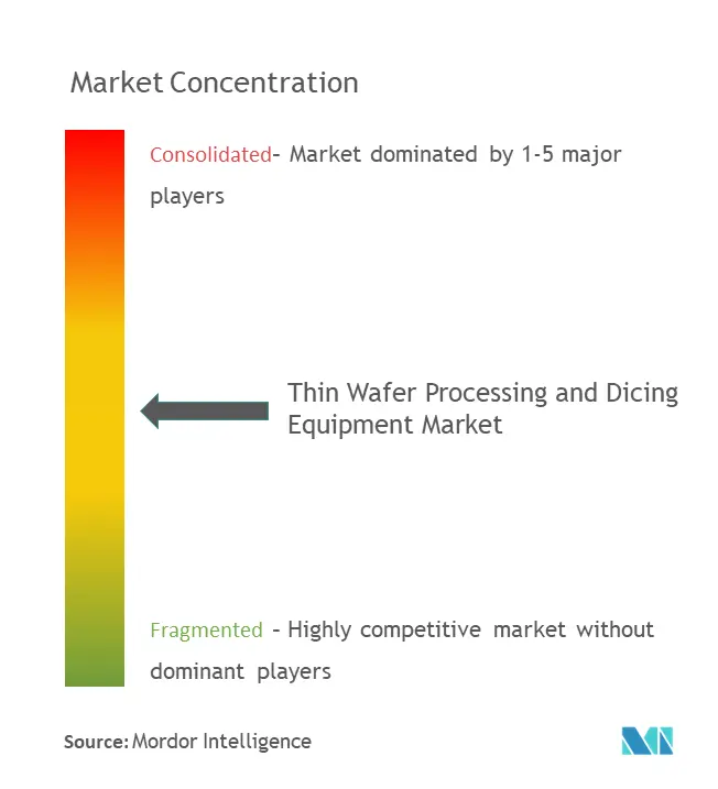
The market for thin wafer processing and dicing comprises very few major players, such as Disco Corporation, Panasonic Corporation, Nippon, and Pulse Motor Taiwan. Moreover, the market still faces considerable challenges in the manufacturing processes of thin wafers. The above-mentioned factor also led to a slower entry of new players into the market. Nevertheless, constant innovations and R&D efforts by the players in the market maintain a competitive edge. Therefore, competitive rivalry in the market at present is rated moderate.
- April 2022 - DISCO Corporation has announced that it has been awarded Intel's EPIC Distinguished Supplier Award. This award distinguishes a consistent level of robust performance across all performance criteria.
- January 2022 - Tokyo-based Yokogawa Electric Corporation signed a memorandum of understanding with Aramco for collaboration to explore potential opportunities for localizing semiconductor chip manufacturing in the Kingdom of Saudi Arabia.
Thin Wafer Processing & Dicing Equipment Market Leaders
-
Suzhou Delphi Laser Co. Ltd
-
SPTS Technologies Limited
-
Plasma-Therm
-
Han's Laser Technology Industry Group
-
ASM Laser Separation International (ALSI) BV
*Disclaimer: Major Players sorted in no particular order
Thin Wafer Processing & Dicing Equipment Market News
- March 2022 - DISCO Corporation has announced the acquisition of real estate in Higashikojiya, Ota-ku, Tokyo. This acquisition of real estate will help the company in its Research and Development growth by using it as an R&D center from April 2022. It will further help the company by supporting the high demand for the semiconductors market in the future.
- March 2022 - DB HiTek announced that the company is planning to replace the old 8-inch wafer equipment with new ones. It is expected to spend a considerable amount on this activity by exceeding the amount it invested in 2021, amounting to KRW 115.2 billion. Also, DB HiTek is planning to boost its 8-inch foundry capacity to 150,000 wafers per month from the current 138,000 wafers per month.
Thin Wafer Processing & Dicing Equipment Market Report - Table of Contents
1. INTRODUCTION
- 1.1 Study Assumptions and Market Definition
- 1.2 Scope of the Study
2. RESEARCH METHODOLOGY
3. EXECUTIVE SUMMARY
4. MARKET INSIGHTS
- 4.1 Market Overview
- 4.2 Introduction to Market Drivers and Restraints
-
4.3 Industry Attractiveness Porter's Five Forces Analysis
- 4.3.1 Threat of New Entrants
- 4.3.2 Bargaining Power of Buyers
- 4.3.3 Bargaining Power of Suppliers
- 4.3.4 Threat of Substitute Products
- 4.3.5 Intensity of Competitive Rivalry
- 4.4 Industry Value Chain Analysis
- 4.5 Assessment of the Impact of COVID-19 on the Market
5. MARKET DYNAMICS
-
5.1 Market Drivers
- 5.1.1 Increasing Demand for Smart Cards, RFID Technology, and Automotive Power ICs
- 5.1.2 Increasing Need for Miniaturization of Semiconductors
-
5.2 Market Restraints
- 5.2.1 Manufacturing Challenges
6. MARKET SEGMENTATION
-
6.1 By Equipment Type
- 6.1.1 Thinning Equipment
- 6.1.2 Dicing Equipment
- 6.1.2.1 Blade Dicing
- 6.1.2.2 Laser Ablation
- 6.1.2.3 Stealth Dicing
- 6.1.2.4 Plasma Dicing
-
6.2 By Application
- 6.2.1 Memory and Logic (TSV)
- 6.2.2 MEMS Devices
- 6.2.3 Power Devices
- 6.2.4 CMOS Image Sensors
- 6.2.5 RFID
- 6.3 By Wafer Thickness Trends
-
6.4 By Wafer Size
- 6.4.1 Less than 4 inch
- 6.4.2 5 inch and 6 inch
- 6.4.3 8 inch
- 6.4.4 12 inch
-
6.5 By Geography
- 6.5.1 North America
- 6.5.1.1 United States
- 6.5.1.2 Canada
- 6.5.2 Europe
- 6.5.2.1 United Kingdom
- 6.5.2.2 Germany
- 6.5.2.3 France
- 6.5.2.4 Spain
- 6.5.2.5 Italy
- 6.5.2.6 Rest of Europe
- 6.5.3 Asia-Pacific
- 6.5.3.1 China
- 6.5.3.2 Japan
- 6.5.3.3 Australia
- 6.5.3.4 India
- 6.5.3.5 Rest of Asia-Pacific
- 6.5.4 Latin America
- 6.5.4.1 Mexico
- 6.5.4.2 Brazil
- 6.5.4.3 Rest of Latin America
- 6.5.5 Middle-East and Africa
- 6.5.5.1 South Africa
- 6.5.5.2 Saudi Arabia
- 6.5.5.3 Rest of Middle-East and Africa
7. COMPETITIVE LANDSCAPE
-
7.1 Company Profiles
- 7.1.1 Suzhou Delphi Laser Co. Ltd
- 7.1.2 SPTS Technologies Limited
- 7.1.3 Plasma-Therm LLC
- 7.1.4 Han's Laser Technology Industry Group Co. Ltd
- 7.1.5 ASM Laser Separation International (ALSI) B.V.
- 7.1.6 Disco Corporation
- 7.1.7 Tokyo Seimitsu Co, Ltd. (Accretech)
- 7.1.8 Neon Tech Co. Ltd.
- 7.1.9 Advanced Dicing Technologies Ltd
- 7.1.10 Panasonic Corporation
- *List Not Exhaustive
8. INVESTMENT ANALYSIS
9. MARKET OPPORTUNITIES AND FUTURE TRENDS
** Subject To AvailablityThin Wafer Processing & Dicing Equipment Industry Segmentation
The need for miniaturization toward small-sized, high-performing, and low-cost device configurations has created the need for thin wafers. Most of which even reached below 100 µm or even 50 µm for applications, such as memory and power devices. Wafers below 390 µm are considered thin wafers. Wafer dicing is the process of separating the die from a semiconductor wafer after the wafer has been processed.
The Thin Wafer Processing and Dicing Equipment is segmented by Equipment Type (Thinning Equipment, Dicing Equipment (Blade Dicing, Laser Dicing, Stealth Dicing, Plasma Dicing)), By Application (Memory and Logic, MEMS Devices, Power Devices, CMOS Image Sensors, RFID), Wafer Thickness, Wafer Size (Less Than 4 Inch, 5 Inch, and 6 Inch, 8 Inch, 12 Inch), and Geography.
| By Equipment Type | Thinning Equipment | |
| Dicing Equipment | Blade Dicing | |
| Laser Ablation | ||
| Stealth Dicing | ||
| Plasma Dicing | ||
| By Application | Memory and Logic (TSV) | |
| MEMS Devices | ||
| Power Devices | ||
| CMOS Image Sensors | ||
| RFID | ||
| By Wafer Size | Less than 4 inch | |
| 5 inch and 6 inch | ||
| 8 inch | ||
| 12 inch | ||
| By Geography | North America | United States |
| Canada | ||
| By Geography | Europe | United Kingdom |
| Germany | ||
| France | ||
| Spain | ||
| Italy | ||
| Rest of Europe | ||
| By Geography | Asia-Pacific | China |
| Japan | ||
| Australia | ||
| India | ||
| Rest of Asia-Pacific | ||
| By Geography | Latin America | Mexico |
| Brazil | ||
| Rest of Latin America | ||
| By Geography | Middle-East and Africa | South Africa |
| Saudi Arabia | ||
| Rest of Middle-East and Africa |
Thin Wafer Processing & Dicing Equipment Market Research FAQs
How big is the Thin Wafer Processing and Dicing Equipment Market?
The Thin Wafer Processing and Dicing Equipment Market size is expected to reach USD 728.39 million in 2024 and grow at a CAGR of 6.35% to reach USD 990.95 million by 2029.
What is the current Thin Wafer Processing and Dicing Equipment Market size?
In 2024, the Thin Wafer Processing and Dicing Equipment Market size is expected to reach USD 728.39 million.
Who are the key players in Thin Wafer Processing and Dicing Equipment Market?
Suzhou Delphi Laser Co. Ltd , SPTS Technologies Limited , Plasma-Therm, Han's Laser Technology Industry Group and ASM Laser Separation International (ALSI) BV are the major companies operating in the Thin Wafer Processing and Dicing Equipment Market.
Which is the fastest growing region in Thin Wafer Processing and Dicing Equipment Market?
Asia Pacific is estimated to grow at the highest CAGR over the forecast period (2024-2029).
Which region has the biggest share in Thin Wafer Processing and Dicing Equipment Market?
In 2024, the Asia Pacific accounts for the largest market share in Thin Wafer Processing and Dicing Equipment Market.
What years does this Thin Wafer Processing and Dicing Equipment Market cover, and what was the market size in 2023?
In 2023, the Thin Wafer Processing and Dicing Equipment Market size was estimated at USD 684.90 million. The report covers the Thin Wafer Processing and Dicing Equipment Market historical market size for years: 2019, 2020, 2021, 2022 and 2023. The report also forecasts the Thin Wafer Processing and Dicing Equipment Market size for years: 2024, 2025, 2026, 2027, 2028 and 2029.
Thin Wafer Processing & Dicing Equipment Industry Report
Statistics for the 2024 Thin Wafer Processing & Dicing Equipment market share, size and revenue growth rate, created by Mordor Intelligence™ Industry Reports. Thin Wafer Processing & Dicing Equipment analysis includes a market forecast outlook to 2029 and historical overview. Get a sample of this industry analysis as a free report PDF download.


