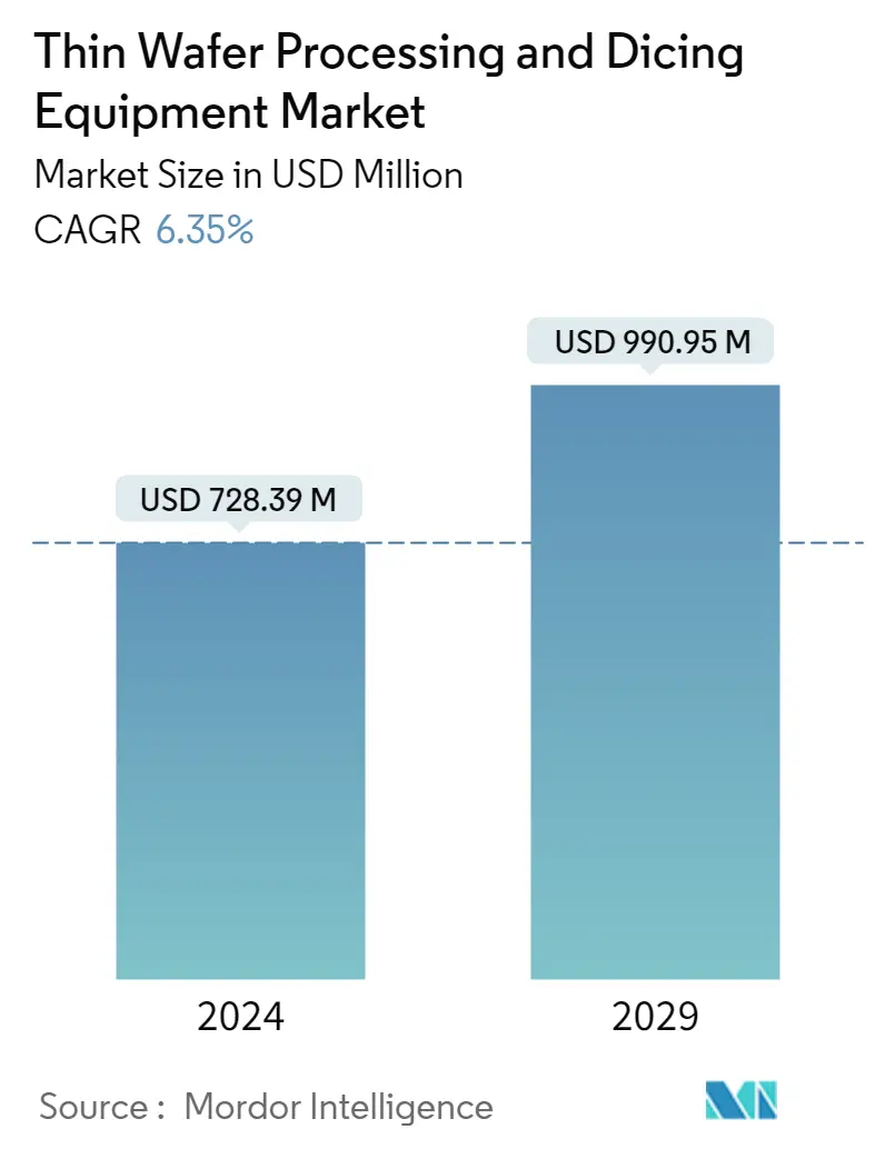
Market Size of Thin Wafer Processing and Dicing Equipment Industry

| Study Period | 2019 - 2029 |
| Market Size (2024) | USD 728.39 Million |
| Market Size (2029) | USD 990.95 Million |
| CAGR (2024 - 2029) | 6.35 % |
| Fastest Growing Market | Asia Pacific |
| Largest Market | Asia Pacific |
Major Players
*Disclaimer: Major Players sorted in no particular order |
Thin Wafer Processing & Dicing Equipment Market Analysis
The Thin Wafer Processing and Dicing Equipment Market size is estimated at USD 728.39 million in 2024, and is expected to reach USD 990.95 million by 2029, growing at a CAGR of 6.35% during the forecast period (2024-2029).
The increasing efforts to make electronic packaging highly resourceful due to the enormous demand for electronic components owing to amplified usage have made electronic packaging useful in a myriad of applications. These factors are driving the growth of the semiconductor and IC packaging market.
- One of the major factors expected to boost the demand for thin wafer processing and dicing equipment in the coming years is the growing demand for three-dimensional integrated circuits, which are widely used in miniature semiconductor devices such as memory cards, smartphones, and smart cards, and various computing devices. Three-dimensional circuits are becoming more popular in multiple space-constrained applications, such as portable consumer electronics, sensors, MEMS, and industrial products because they improve overall product performance in terms of speed, durability, low power consumption, and lightweight memory.
- The expanding use of server and data center systems across various enterprises and industries, due to the widespread availability of low-cost cloud computing solutions, is likely to fuel demand for logic devices like microprocessors and digital signal processors. In addition, as the number of IoT-enabled linked devices grows, the utilization of microprocessors also increases. Thin wafers are increasingly employed in these devices to enable effective temperature management and enhance performance. All of these reasons are assisting in expanding the logic device market.
- Silicon wafers have long been used as a fabrication platform in microelectronics and MEMS. The silicon-on-insulator substrate is a unique variation of the standard silicon wafer. Two silicon wafers are glued together using a bond layer of silicon dioxide with a thickness of about 1-2 m to make these wafers. One silicon wafer gets flattened down to 10-50 m in thickness. The application will determine the exact thickness of the coating.
- The cost of building state-of-the-art thin wafer foundries has increased exponentially, which puts pressure on the industry. This is where the number of semiconductor manufacturers was consolidated in recent times. Performance boosts are slowing down, making specialized thin wafers increasingly attractive. The design decisions that enable thin wafers to be universal may be sub-optimal for some computing tasks.
- Due to the global slowdown in demand in the industrial and automotive electronics sectors that the COVID-19 pandemic has worsened, manufacturers operating in the market have registered a decline in orders for Thin Wafer semiconductors.
Thin Wafer Processing & Dicing Equipment Industry Segmentation
The need for miniaturization toward small-sized, high-performing, and low-cost device configurations has created the need for thin wafers. Most of which even reached below 100 µm or even 50 µm for applications, such as memory and power devices. Wafers below 390 µm are considered thin wafers. Wafer dicing is the process of separating the die from a semiconductor wafer after the wafer has been processed.
The Thin Wafer Processing and Dicing Equipment is segmented by Equipment Type (Thinning Equipment, Dicing Equipment (Blade Dicing, Laser Dicing, Stealth Dicing, Plasma Dicing)), By Application (Memory and Logic, MEMS Devices, Power Devices, CMOS Image Sensors, RFID), Wafer Thickness, Wafer Size (Less Than 4 Inch, 5 Inch, and 6 Inch, 8 Inch, 12 Inch), and Geography.
| By Equipment Type | ||||||
| Thinning Equipment | ||||||
|
| By Application | |
| Memory and Logic (TSV) | |
| MEMS Devices | |
| Power Devices | |
| CMOS Image Sensors | |
| RFID |
| By Wafer Size | |
| Less than 4 inch | |
| 5 inch and 6 inch | |
| 8 inch | |
| 12 inch |
| By Geography | ||||||||
| ||||||||
| ||||||||
| ||||||||
| ||||||||
|
Thin Wafer Processing and Dicing Equipment Market Size Summary
The Thin Wafer Processing and Dicing Equipment Market is poised for significant growth, driven by the increasing demand for compact and efficient electronic devices. This demand is largely fueled by the rise of three-dimensional integrated circuits, which are essential for enhancing the performance of miniature semiconductor devices used in smartphones, memory cards, and various computing devices. The market is also benefiting from the expanding use of server and data center systems, propelled by the availability of cost-effective cloud computing solutions. As the number of IoT-enabled devices continues to rise, the need for thin wafers to improve temperature management and performance in these devices is becoming more pronounced. Despite challenges such as the high cost of establishing advanced thin wafer foundries and the global slowdown in demand due to the COVID-19 pandemic, the market is expected to experience a robust growth trajectory.
Regionally, the Asia Pacific stands out as the largest and fastest-growing semiconductor market, with countries like China, South Korea, and Singapore driving demand for consumer electronics. The region's growth is supported by strategic acquisitions and government incentives, particularly in China, which has seen a rise in market players focusing on expansion through mergers and acquisitions. Japan remains a key player in the semiconductor industry, with significant contributions from major manufacturers and suppliers of critical materials. Meanwhile, initiatives like the Quad Alliance's semiconductor supply chain project aim to enhance supply chain security and capacity in the Asia Pacific. In India, government efforts to develop a self-sufficient semiconductor ecosystem are underway, further bolstering the market's growth prospects. Despite the presence of few major players and challenges in manufacturing processes, ongoing innovations and research and development efforts are maintaining a competitive edge in the market.
Thin Wafer Processing and Dicing Equipment Market Size - Table of Contents
-
1. MARKET INSIGHTS
-
1.1 Market Overview
-
1.2 Introduction to Market Drivers and Restraints
-
1.3 Industry Attractiveness Porter's Five Forces Analysis
-
1.3.1 Threat of New Entrants
-
1.3.2 Bargaining Power of Buyers
-
1.3.3 Bargaining Power of Suppliers
-
1.3.4 Threat of Substitute Products
-
1.3.5 Intensity of Competitive Rivalry
-
-
1.4 Industry Value Chain Analysis
-
1.5 Assessment of the Impact of COVID-19 on the Market
-
-
2. MARKET SEGMENTATION
-
2.1 By Equipment Type
-
2.1.1 Thinning Equipment
-
2.1.2 Dicing Equipment
-
2.1.2.1 Blade Dicing
-
2.1.2.2 Laser Ablation
-
2.1.2.3 Stealth Dicing
-
2.1.2.4 Plasma Dicing
-
-
-
2.2 By Application
-
2.2.1 Memory and Logic (TSV)
-
2.2.2 MEMS Devices
-
2.2.3 Power Devices
-
2.2.4 CMOS Image Sensors
-
2.2.5 RFID
-
-
2.3 By Wafer Thickness Trends
-
2.4 By Wafer Size
-
2.4.1 Less than 4 inch
-
2.4.2 5 inch and 6 inch
-
2.4.3 8 inch
-
2.4.4 12 inch
-
-
2.5 By Geography
-
2.5.1 North America
-
2.5.1.1 United States
-
2.5.1.2 Canada
-
-
2.5.2 Europe
-
2.5.2.1 United Kingdom
-
2.5.2.2 Germany
-
2.5.2.3 France
-
2.5.2.4 Spain
-
2.5.2.5 Italy
-
2.5.2.6 Rest of Europe
-
-
2.5.3 Asia-Pacific
-
2.5.3.1 China
-
2.5.3.2 Japan
-
2.5.3.3 Australia
-
2.5.3.4 India
-
2.5.3.5 Rest of Asia-Pacific
-
-
2.5.4 Latin America
-
2.5.4.1 Mexico
-
2.5.4.2 Brazil
-
2.5.4.3 Rest of Latin America
-
-
2.5.5 Middle-East and Africa
-
2.5.5.1 South Africa
-
2.5.5.2 Saudi Arabia
-
2.5.5.3 Rest of Middle-East and Africa
-
-
-
Thin Wafer Processing and Dicing Equipment Market Size FAQs
How big is the Thin Wafer Processing and Dicing Equipment Market?
The Thin Wafer Processing and Dicing Equipment Market size is expected to reach USD 728.39 million in 2024 and grow at a CAGR of 6.35% to reach USD 990.95 million by 2029.
What is the current Thin Wafer Processing and Dicing Equipment Market size?
In 2024, the Thin Wafer Processing and Dicing Equipment Market size is expected to reach USD 728.39 million.

